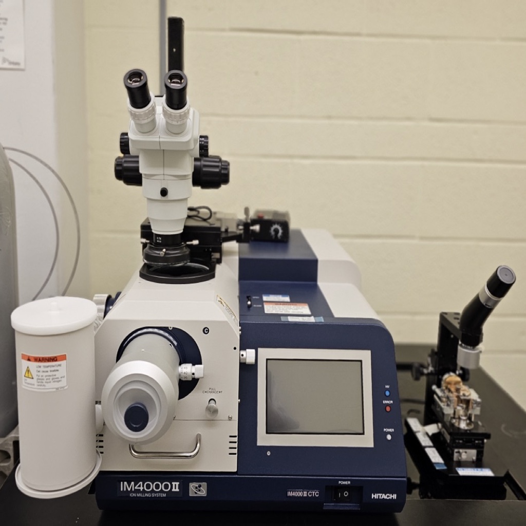
Hitachi S-4800 High Resolution SEM
As of November 2021, the Hitachi S4800 now has powerful EDS capability with the installation of Oxford’s Ultim Max 100mm2 large area silicon drift detector. It allows video rate electron and chemical imaging in real time with live tracing features to remember where you already looked and what elements were located there. MRL users can be trained to operate the instrument or have staff assist in collecting the images for them as requested. Before using the instrument, users are given access to video instruction on the fundamental theory behind the SEM technique to better understand instrument operation and data interpretation. Users are first trained on sample preparation including sputter coating if necessary. They are then instructed in safe instrument operation including sample loading, instrument alignment, and sample imaging. The best conditions for each unique sample are determined in the training session. Below are pictures of a sample holder and types of sample mounts available for the Hitachi 4800 SEM.
Capabilities
- ✓High Resolution Low Voltage imaging 1.0 nm resolution at 15 kV, WD=4mm 1.4 nm resolution at 1 kV, WD=1.5nm, Deceleration mode 2.0 nm resolution at 1 kV, WD=1.5mm, Normal mode
- ✓1.0 nm resolution at 15 kV, WD=4mm
- ✓1.4 nm resolution at 1 kV, WD=1.5nm, Deceleration mode
- ✓2.0 nm resolution at 1 kV, WD=1.5mm, Normal mode
- ✓Beam deceleration (ultra-low landing voltages (100-500 V) for shallow surface topography)
- ✓Controlled signal mixing (combination of secondary electron and back scattered electron)
- ✓Pure BSE imaging at low voltages
- ✓Electron gun – cold field emission type
- ✓High magnification mode 100x to 800,000x
- ✓Low magnification mode 30x to 2,000x
- ✓Accelerating Voltage range 0.5 to 30 kV in 100V steps
- ✓Maximum sample size 4 inches in diameter
- ✓Location 0013 Supercon
- ✓Related Research Techniques Scanning Electron Microscopy (SEM)
- ✓Related Research Cores Electron Microscopy (EM)


